How to Budget Loss and Impedance for Multi Layer PCB Stacks
Loss and impedance are two sides of the same stackup. Dielectric height and Er set each layer's impedance, and the same numbers, plus copper, set its loss per inch. Budget them together and you avoid a stackup that hits 50 Ω but still runs out of dB.
Step 1: Break the channel into parts
Start from the interface budget at Nyquist, say 28 dB at 8 GHz for PCIe Gen4, and keep a design margin of 2 to 3 dB. Then list every part between transmitter and receiver: packages, board routes, vias, connectors and cables.
Fixed parts like packages and connectors come from datasheets. Routes depend on length and laminate.

FlowSimLab's Channel step adds the parts up as you go. Here the two packages, 11 inches of route, four vias and a CEM connector total 16.2 dB.
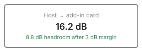
The same panel also works out the longest PCB route the budget allows, here 20.75 inches. That is the number layout needs before routing begins.
Step 2: Know which layer each route uses
Outer-layer microstrip and inner-layer stripline behave differently. Microstrip has part of its field in air, so its effective Er and delay are lower, but solder mask and surface finish affect it. Stripline is fully embedded, more predictable and better shielded, but slightly lossier per inch at the same impedance because it runs narrower.
In the Layers step, every signal layer should sit next to a solid reference plane, and the total thickness should land on target.
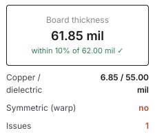
The same panel warns about asymmetric stackups, which bow and twist during reflow.
Step 3: Set impedance per layer
With the stackup fixed, solve the trace width for the target impedance on each signal layer, using the real Er, dielectric height and copper weight. Keep a tolerance, usually ±10%, and note the delay and loss per inch while you are there.
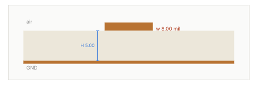
FlowSimLab's trace step has a Solve width action for the target impedance and reports effective Er, delay, loss split into dielectric and copper, and reflection against the termination.
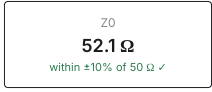
Saved trace types are linked to the routes in your channel by name, so the standards check can compare their impedance with the interface target.
Step 4: Close the loop
If the budget is tight, the levers are clear: a lower-loss laminate, smoother copper, wider traces on thicker dielectric, shorter routes or fewer vias. Each one moves loss per inch, impedance, or both. That is why budget and stackup should be revisited together, not one after the other.
Summary
- Budget loss part by part, and derive the maximum PCB length.
- Put every fast layer next to a solid reference.
- Solve width per layer for impedance, and note loss per inch.
- Iterate laminate, copper and geometry until both budgets close with margin.
Choosing the laminate itself is covered in A Practical Guide to Laminate Selection for PCIe and Ethernet Interfaces. For the reasoning behind the closed-form numbers, see Using Analytical Formulas for High-Speed Interconnects.