How to Use Standards Checks to Accelerate PCB Sign Off
PCB sign-off is slow for one main reason: it is the first time all the decisions are looked at together. A laminate chosen in week one, a budget written on a whiteboard, a stackup changed for cost in week six. Standards checks bring those decisions together continuously, so sign-off becomes a confirmation rather than an investigation.
Why sign-off takes so long
Think about how a typical high-speed board reaches review. The interfaces were chosen early: a couple of PCIe links, some Ethernet lanes, a memory bus. Each one comes with a specification that sets limits on loss, impedance and, in practice, on materials and stackup.
Then the design moves on. The laminate is picked from what the fab stocks. Someone builds a loss spreadsheet for the longest channel. The stackup is drawn, then redrawn to save a layer. Trace widths are solved by a field solver for one layer and copied to another. The ball map is negotiated with the package team.
None of these steps is wrong. The trouble is that each one is checked against the interface only once, if at all, and usually by a different person. By the time the board reaches sign-off, the reviewer has to rebuild the whole chain to answer a simple question: does every channel still meet its standard?
That rebuild is the slow part. It means hunting down the current stackup file, finding which version of the budget spreadsheet is the latest, re-solving impedance for the layers that changed, and digging through the spec for the right limit. When something fails, the fix often ripples back through decisions made weeks earlier.
Standards checks shorten this by doing the comparison continuously, from the same data the design is built on.
What a standards check actually is
A standards check is a simple comparison: one number from your design against one limit from the interface specification. Its value is not in the arithmetic, which is easy. It is in doing the comparison automatically, every time something changes, using the design's real values rather than a copy.
For high-speed channels, four checks cover most of what goes wrong:
- Insertion loss: does the total channel loss at Nyquist fit inside the interface budget, with margin?
- Impedance: do the board routes land on the interface's impedance target, within tolerance?
- Material: is the laminate's loss in the right class for the interface's Nyquist frequency?
- Return path: does every signal layer sit next to a solid reference plane?
There are more you could add: crosstalk, skew, via stub resonance, return loss. But these four catch the majority of late surprises, and they are cheap to run because they only need data the design already has.
The interface limits
Every check needs a limit, and the limit comes from the interface. FlowSimLab keeps a table of typical values for common interfaces, highlighted for the ones your project uses.
| Interface | Signalling | Nyquist | IL budget | Diff. impedance | Laminate guideline |
|---|---|---|---|---|---|
| PCIe Gen3 (8 GT/s) | NRZ | 4.00 GHz | 22 dB | 85 Ω ±15% | Df ≤ 0.02 |
| PCIe Gen4 (16 GT/s) | NRZ | 8.00 GHz | 28 dB | 85 Ω ±15% | Df ≤ 0.012 |
| PCIe Gen5 (32 GT/s) | NRZ | 16.00 GHz | 36 dB | 85 Ω ±15% | Df ≤ 0.005 |
| PCIe Gen6 (64 GT/s) | PAM4 | 16.00 GHz | 32 dB | 85 Ω ±15% | Df ≤ 0.005 |
| 10GBASE-KR | NRZ | 5.16 GHz | 25 dB | 100 Ω ±10% | Df ≤ 0.012 |
| 25GBASE-KR / 100G-KR4 | NRZ | 12.89 GHz | 35 dB | 100 Ω ±10% | Df ≤ 0.008 |
| 100G per lane PAM4 | PAM4 | 26.56 GHz | 28 dB | 100 Ω ±10% | Df ≤ 0.003 |
Two notes on this table. First, the budgets are typical bump-to-bump values. They vary by specification revision and by how a given spec splits the budget between host, connector and add-in card, so always confirm against the revision you design to. Second, the laminate column is a rule of thumb, not a spec limit. No standard says "use this material". It is a guideline derived from the Nyquist frequency, and it is there to warn early, not to fail a design.
The Nyquist frequency itself is worth a second look. For NRZ it is half the bit rate. For PAM4 each symbol carries two bits, so Nyquist is a quarter of the bit rate. That is why PCIe Gen5 at 32 GT/s NRZ and Gen6 at 64 GT/s PAM4 share the same 16 GHz Nyquist. The material requirements are almost identical; the budget and the eye margin are what tighten.
Check 1: Insertion loss
The insertion-loss check compares the channel's total loss at Nyquist with the interface budget.
The total comes from the channel itself. In FlowSimLab that is the Channel step, where each link is listed part by part from transmitter to receiver: packages, PCB routes, vias, connectors and cables. Fixed parts take a loss in dB; routes take a length and use the project laminate's loss per inch at Nyquist.
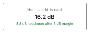
The check has three outcomes, and the middle one matters most:
- Pass: total loss is below the budget minus your chosen margin.
- Check: total loss is inside the budget but has eaten into the margin.
- Fail: total loss exceeds the budget.
The margin is yours to set, typically 2 to 3 dB. It covers what the closed-form numbers do not: manufacturing tolerance, temperature, aging and the gap between simulation and measurement. A channel that lands inside the margin is not broken, but it is one surprise away from failing, and it deserves a look before layout is frozen.
How the budget is built in detail is covered in How to Budget Loss and Impedance for Multi Layer PCB Stacks.
Check 2: Impedance
The impedance check compares each PCB route in the channel with the interface's impedance target.
Most high-speed interfaces specify a differential impedance: 85 Ω for PCIe, 100 Ω for backplane Ethernet. FlowSimLab's first-order check compares single-ended trace impedance with half of that, so 42.5 Ω for PCIe and 50 Ω for Ethernet, within the interface tolerance. That assumes a loosely coupled pair, where the differential impedance is close to twice the single-ended value. Tightly coupled pairs drop below that, which is why this check is a first pass and the final pair geometry should still be solved properly.
The link between the channel and the trace is the name. Each PCB route in the Channel step should have a trace type of the same name in the Single-ended trace step. When it does, the check reads that trace type's topology, Er, dielectric height, width and copper weight, computes its impedance and compares it with the target.
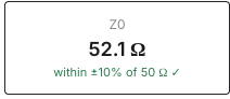
When a route has no matching trace type, the check does not guess. It flags the route for review and says why, for example "Host board route: no trace type". That is deliberately a check rather than a fail: nothing is known to be wrong, but nothing has been confirmed either.
Check 3: Material
The material check compares the project laminate's Df with the guideline for the channel's Nyquist frequency.
The guideline steps up as frequency rises:
- Up to 4 GHz: Df ≤ 0.02, standard FR4.
- Up to 8 GHz: Df ≤ 0.012, mid loss.
- Up to 13 GHz: Df ≤ 0.008, low loss.
- Up to 16 GHz: Df ≤ 0.005, very low loss.
- Above 16 GHz: Df ≤ 0.003, ultra-low loss.
Because this is a rule of thumb, a laminate above the guideline is flagged as a check, never a fail. A short route on a slightly lossier material can still close its budget comfortably; the insertion-loss check is the one that decides. The material check simply makes sure nobody is surprised.
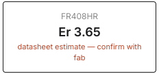
Choosing the laminate in the first place is covered in A Practical Guide to Laminate Selection for PCIe and Ethernet Interfaces, including how to compare two candidates on a spider chart.
Check 4: Return path
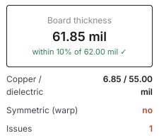
The return-path check looks at the stackup rather than at any one channel. It asks whether every signal layer sits directly next to a ground or power plane.
A signal's return current flows in the nearest plane, right underneath the trace. If there is no adjacent plane, the return current spreads out, loop inductance rises, impedance becomes hard to control and crosstalk goes up. This is one of the oldest rules in high-speed layout, and one of the easiest to break when a stackup is reworked to save a layer.
Unlike the other three, this check does fail outright. A signal layer with no adjacent plane is a structural problem, and it names the offending layers so they are easy to find.
Reading the results
FlowSimLab shows the checks as one row per channel, with a column for each check and a pill that says Pass, Check or Fail, along with the value and a short reason.

Read a row left to right and it tells a short story. In the example above, a host-to-add-in-card link on PCIe Gen4 uses 16.2 of its 28 dB, leaving 11.8 dB spare. The laminate, at Df 0.0094, sits inside the mid-loss guideline. All three signal layers are next to a plane. The only open item is impedance, because the two routes have not yet been linked to trace types.
A summary line above the table counts everything up.

That count is a useful health signal for a project. Zero fails is the minimum for sign-off. Every check either gets resolved or gets a written explanation.
Using checks to move faster
The checks are only useful if they change how the work is done. Here is how they speed things up in practice.
Run them from day one
The checks need very little to start. A material, one channel and a stackup are enough for three of the four. Open the Standards step as soon as you have them, and keep it open as the design develops. A fail on day three costs a conversation; the same fail at sign-off costs a respin of the stackup.
Treat "check" as a to-do list
Every "check" is a specific, small task: link a route to a trace type, confirm a laminate is acceptable on a short route, decide whether to spend margin. Working through them as they appear keeps the list short. At sign-off, the remaining items should be the ones you chose to accept, each with a reason.
Ask "what if" before the meeting
Because the checks are recalculated whenever an input changes, they are a fast way to answer what-if questions.
Take the same PCIe channel and change its interface from Gen4 to Gen5. The budget rises from 28 to 36 dB, but Nyquist doubles to 16 GHz, so every route gets lossier.

The result is instructive. Insertion loss still passes, at 22.5 dB with 13.5 dB spare, because this link is short. But the laminate is now flagged, because Df 0.0094 is above the 0.005 guideline for 16 GHz. The honest conclusion is not "change material". It is "this short link can stay on the mid-loss laminate; longer Gen5 links in the same board may not". That is a five-second answer to a question that usually takes a meeting.
Keep one source of truth
The biggest time saver is not the arithmetic; it is that every check reads from the same project data as the design. There is no separate spreadsheet to keep in sync. When the stackup changes in the Layers step, the return-path check updates. When a route gets longer in the Channel step, insertion loss updates. When the laminate changes, both the material check and every route's loss update.
Hand over a readable record
At sign-off, the Standards step is the summary. One row per channel, four checks each, with values and reasons. Reviewers can see what was checked and what was accepted without reconstructing the design. Paired with the full high-speed channel checklist, it covers most of what a design review needs.
A worked example
Here is how the checks shape a small project from start to finish.
The board has one PCIe Gen4 link from a host processor through a CEM connector to an add-in card, plus a 10GBASE-KR lane to a backplane connector. The fab offers FR4, FR408HR and Megtron 6.
Day one. The team enters the requirements in the Material step: 16 GT/s NRZ as the fastest rate, a 10 inch longest route, an 8 layer board, lead-free assembly. FR408HR is chosen for cost and thermal reasons. The PCIe channel is entered in the Channel step with two packages, an 8 inch host route, four breakout vias, the CEM connector and a 3 inch add-in route. A default 6 layer stackup is in place.
The Standards step shows one row: insertion loss, material and return path pass; impedance is flagged because there are no trace types yet.
Day two. The team defines the host and add-in routes as trace types in the Single-ended trace step, named to match the channel. The impedance check now computes each route against 42.5 Ω and passes. The 10GBASE-KR channel is added. Its row passes insertion loss and material, and flags impedance until its route is defined against the 50 Ω target.
Week two. To save cost, someone proposes swapping a plane for an extra signal layer. In the Layers step, the change is made as an experiment, and the return-path check fails at once, naming the signal layer that no longer has an adjacent plane. The experiment is reverted before anyone spends time on routing.
Week three. A product manager asks whether the same board could support PCIe Gen5 later. The interface is switched to Gen5 for a moment. Insertion loss still passes on this short link, but the material check flags FR408HR against the very-low-loss guideline. The answer goes back the same day: yes for this link, with a note that a longer Gen5 link would need a better laminate.
Sign-off. Every row shows zero fails. The only remaining checks have written explanations. The review takes an hour instead of a week, because nothing needs to be rebuilt.
What standards checks do not replace
It is important to be clear about the limits.
The checks are first-order. Insertion loss uses closed-form loss per inch and datasheet part values, not a full-wave extraction. Impedance assumes a loosely coupled pair. The laminate guideline is a rule of thumb. All of these are good enough to steer a design and catch mistakes early. None of them replaces a detailed channel simulation, a compliance test or first-article measurements.
Think of them as a fast, always-on filter. They make sure that what reaches detailed simulation is already close to right, and that the expensive analysis is spent confirming a good design rather than discovering a broken one. When the detailed results come back, simulation versus measurement correlation is the next place to look. For background on where closed-form models hold and where they do not, see Using Analytical Formulas for High-Speed Interconnects.
Getting started
If you want to try this on your own design, the order is simple:
- Set the project material in step 1.
- Add each channel in step 2 and choose its interface.
- Define each PCB route as a trace type in step 3, named to match.
- Build the stackup in step 5.
- Open the Standards step and keep it open.
The dashboard walks through these steps in order, and Step by Step Channel Setup Using FlowSimLab DSS for High Speed Designs covers each one in detail.
Summary
- Sign-off is slow because it is the first time decisions are checked together.
- Four checks catch most problems: insertion loss, impedance, material and return path.
- Run them from day one, on the same data the design is built from.
- Treat "check" as a to-do list and "fail" as a stop sign.
- Use them for what-if questions before meetings, not after.
- Remember they are first-order; detailed simulation and measurement still confirm the design.
Done this way, sign-off stops being an investigation and becomes a read-back of decisions that were already checked. To see it on your own board, talk to our team.