Chip Packaging Transitions from Package to Board Explained
The package-to-board transition is often the worst-behaved part of a channel. It packs several impedance changes into a few millimetres, sits right next to the transmitter or receiver where reflections hurt most, and is usually designed by two teams who rarely share a model.
The path, step by step
A high-speed signal typically crosses five transitions before it reaches a board trace:
- Die to package, through a wire bond or a flip-chip bump.
- Package routing, through traces and micro-vias in the substrate.
- Package to board, through a solder ball and its land.
- Breakout, through the via from the ball pad down to the routing layer.
- The first trace segment, often necked down under the BGA.
Each of these has its own geometry and its own impedance. None of them is 50 Ω or 85 Ω by default. They have to be designed that way.
Where it goes wrong
Wire bonds add inductance
A bond wire is a thin conductor in air. As a rule of thumb it adds about 1 nH per millimetre, and its reactance grows with frequency. At a few GHz, a long single bond acts like a series inductor big enough to reflect and roll off the signal.
Shorter loops, lower loop heights and parallel bonds all help. The Wire Bond explorer in FlowSimLab ranks bond geometries by inductance.
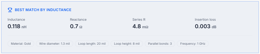
Even that small 0.118 nH grows from 0.7 Ω of reactance at 1 GHz to about 30 Ω at 40 GHz. Flip-chip bumps are far shorter, which is one reason they dominate high-speed packages.
Balls and pads add capacitance
A BGA ball and its pads are wide compared with the trace that follows. Wide metal close to a plane means extra capacitance and a dip in impedance. Smaller pads, or plane cut-outs under the pad, compensate for it.
Breakout vias add stubs
The breakout via is the first vertical step on the board. If it is a through-hole via and the signal exits on an upper layer, the rest of the barrel is a stub that resonates near a quarter wavelength. The return current also has to jump between planes; without a nearby ground ball or stitching via, it takes the long way round. Via choices are covered in more depth in Choosing Vias and Connectors for High Speed Data Paths.
Ball assignment decides crosstalk
Which balls carry signal, ground and power matters as much as their shape. A signal-to-ground ratio of 1:1 gives every signal its own return. Ratios of 2:1 or 3:1 save balls but raise crosstalk and loop inductance.
How FlowSimLab handles the transition
The Bumps step works from the net groups and stackup you already defined, so the package is designed against the real board, not in isolation.
You set the grid (rows, columns and pitch) and a signal-to-ground pattern. Auto-assign places your groups using that pattern, or you paint nets, ground and power by hand. A running summary keeps count of signal, ground and power bumps, the actual signal-to-ground ratio, and the worst via stub.
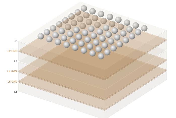
Switch the 3D view to bump-to-layer and each signal is drawn from its bump down to the layer its group was assigned to, using through, back-drilled, blind or stacked micro-via styles. Long stubs show up immediately, not after a field solve.
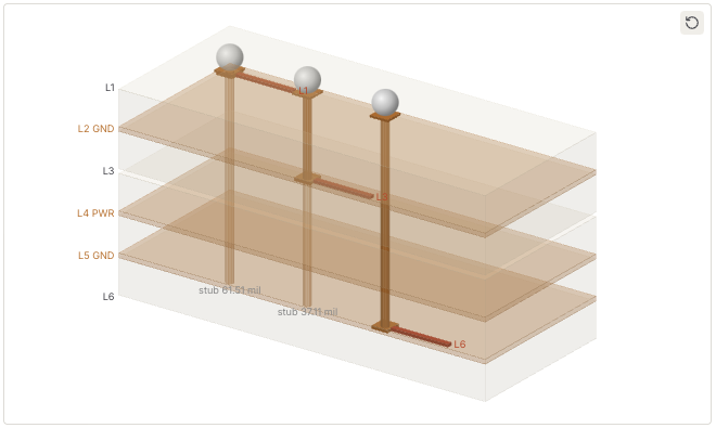
In this six-layer example the stubs are 61.51 mil and 37.11 mil, which resonate near 25 GHz and 42 GHz on FR408HR. That is fine for a 16 GT/s link and a warning for 56 Gbaud. Moving the fastest groups to lower layers, or switching to back-drilled vias, is a quick change you can see at once.
Practical guidelines
- Keep bond wires short and low; use parallel bonds for fast or high-current nets.
- Give every high-speed signal ball an adjacent ground ball.
- Compensate pad capacitance with plane cut-outs where your fab allows.
- Put the fastest groups on layers that minimise via stub, or backdrill.
- Check the whole path from bump to routing layer before freezing the ball map.
The package-to-board transition is short, but it is where the transmitter first meets the board. Designing it against the real stackup removes most late surprises. To see where this step sits in the full flow, read Step by Step Channel Setup Using FlowSimLab DSS for High Speed Designs.