Choosing Vias and Connectors for High Speed Data Paths
In a high-speed path, the via and the connector are the discontinuities. Each one is short, but each changes impedance and can add a resonance. Choosing them well is less about finding a perfect part and more about avoiding the two or three mistakes that close an eye.
What makes a via good or bad
A signal via is a short vertical transmission line. It has a pad at each end, an anti-pad in every plane it crosses and, ideally, a ground via close by to carry the return current.
Its impedance comes mostly from drill and pad size against anti-pad clearance. Oversized pads add capacitance, and so do undersized anti-pads. A distant return via adds loop inductance and lets energy leak into the plane cavity.
Then there is the stub. When a through-hole via carries a signal from L1 to L3, the barrel below L3 is an open-ended stub. It resonates near a quarter wavelength:
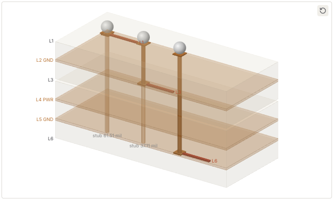
On FR408HR, a 61.5 mil stub resonates near 25 GHz and a 37 mil stub near 42 GHz. That is comfortable for a 5 GHz Nyquist and a real risk for 112G PAM4. Backdrilling, blind vias, or routing fast signals on layers near the far side all shorten the stub.
What makes a connector good or bad
For connectors the questions are simpler. Is it rated above your frequency? What is its return loss across the band? How much loss does it add?
The board launch matters as much as the connector body, because the footprint is part of the discontinuity. In a typical budget a connector costs 1 to 2 dB at Nyquist, so it deserves as much attention as an inch of trace.
Finding a matching part in FlowSimLab
The component library covers vias, microstrip, grounded CPW, stripline, wire bonds and coaxial connectors. Each part has filterable geometry and a large set of pre-computed datasets.
In the Signal Via explorer you can constrain via type, substrate, drill, pad, anti-pad, plating, return-via spacing, dielectric and frequency, then rank the results.
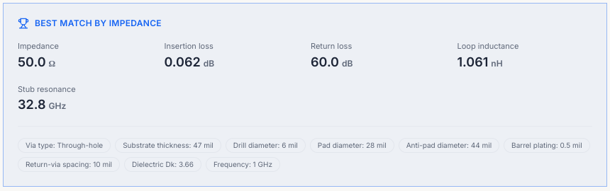
Rank by stub resonance instead and the question changes to: which geometry pushes the resonance furthest from my band?
The connector explorer works the same way across SMA, 2.92, 2.4 and 1.85 mm series, launch style, gender and dielectric.
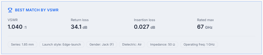
Whatever you pick, its loss goes into the Channel step as a part in the transmitter-to-receiver chain, so the budget always reflects the real hardware.
Quick rules
- Keep a ground via close to every signal via that changes reference.
- Size anti-pads for impedance, not just clearance.
- Calculate stub resonance and keep it well above Nyquist; backdrill if it is not.
- Choose connectors rated above your band, and check the launch, not only the part.
Library metrics are closed-form approximations, so validate critical geometries with a full-wave solve. Our note on using analytical formulas for high-speed interconnects covers where those formulas hold. For the transition before the via, from chip to board, read Chip Packaging Transitions from Package to Board Explained.